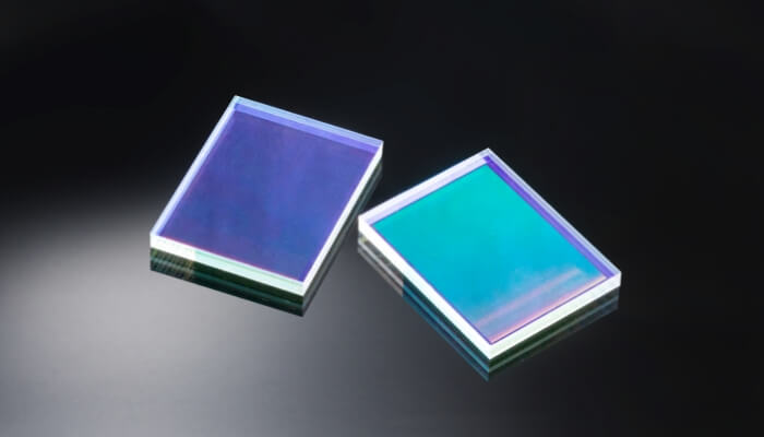
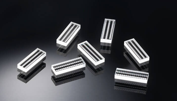
Micro Lens Array (MLA)
We produce microstructures on glass or silicon substrate using NSG’s unique organic–inorganic hybrid material to provide diverse micro optical elements with superior productivity and reliability.


Product summary
Microlens is a minute lens whose diameter is a few dozen to a few hundred micrometers. In optical communication, it is used to gather lights emitted from the light sources and efficiently couple them at the optical fiber core or the receiver of the sensor, and in optical sensing, it is used to widen light in a given angle and strength distribution and illuminate the target area. Lens array is a type of optical element where lenses are arranged in a sequence. NSG is capable of accommodating various demands including the shapes of the lenses, size, number and arrangement. These micro optical elements are used in fields such as medicine, automobile and factory automation, in addition to optical communication and IT.
Features of microlens array
(1) We can provide diverse types of lenses and optical elements utilizing our optical design technologies acquired through experience in development and production of optronics-related products.
(2) We achieve high reliability and thermal resistance that comply with the Telcordia Standard and accommodate reflow temperature above 300℃ through the organic‐inorganic hybrid technology.
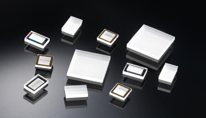
(3) Using the unique process of NSG, we are capable of precision alignment to substrate up to 8 inches and formation of partial microstructure on substrates.
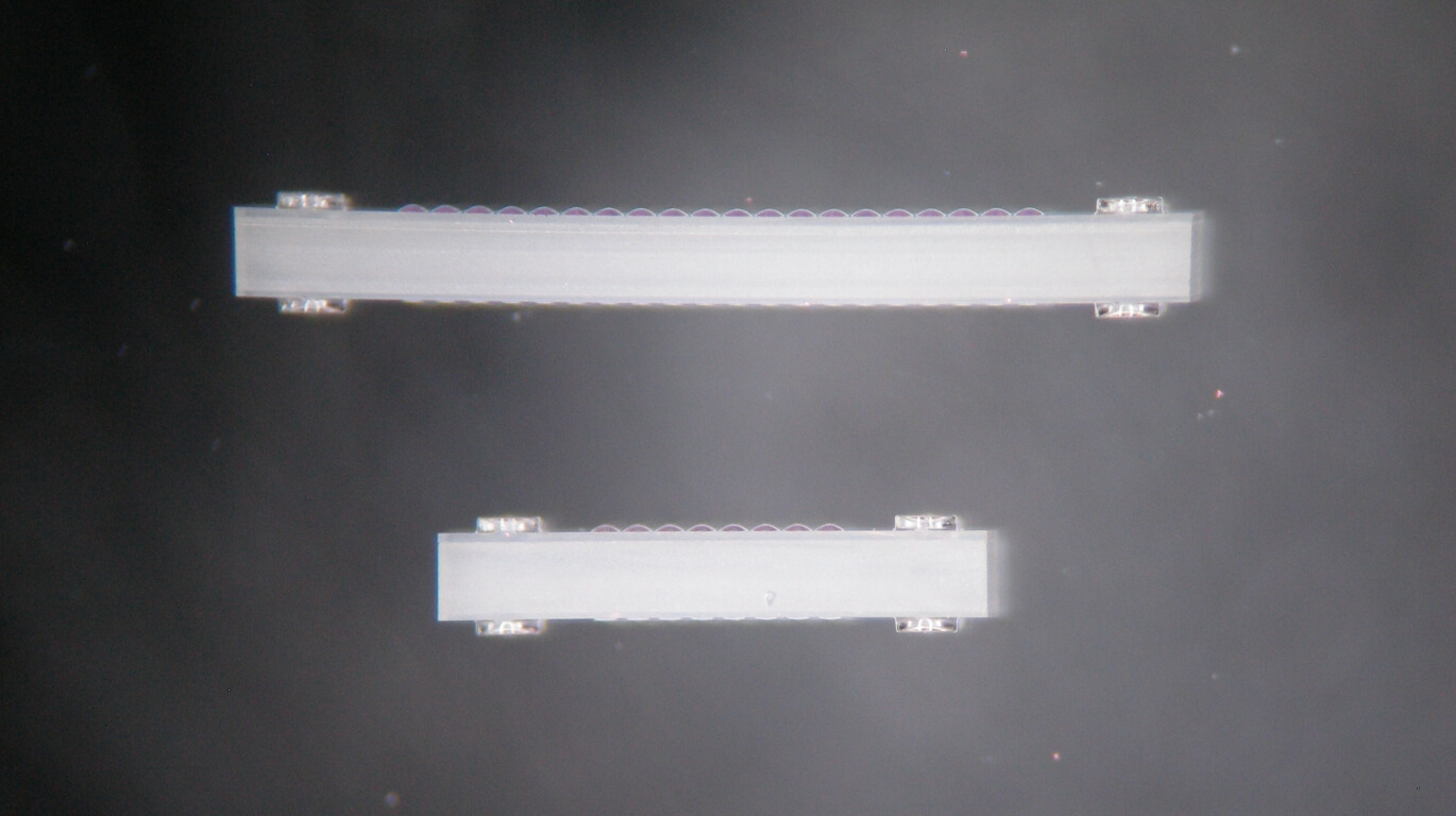
Precision alignment (double-sided lens)
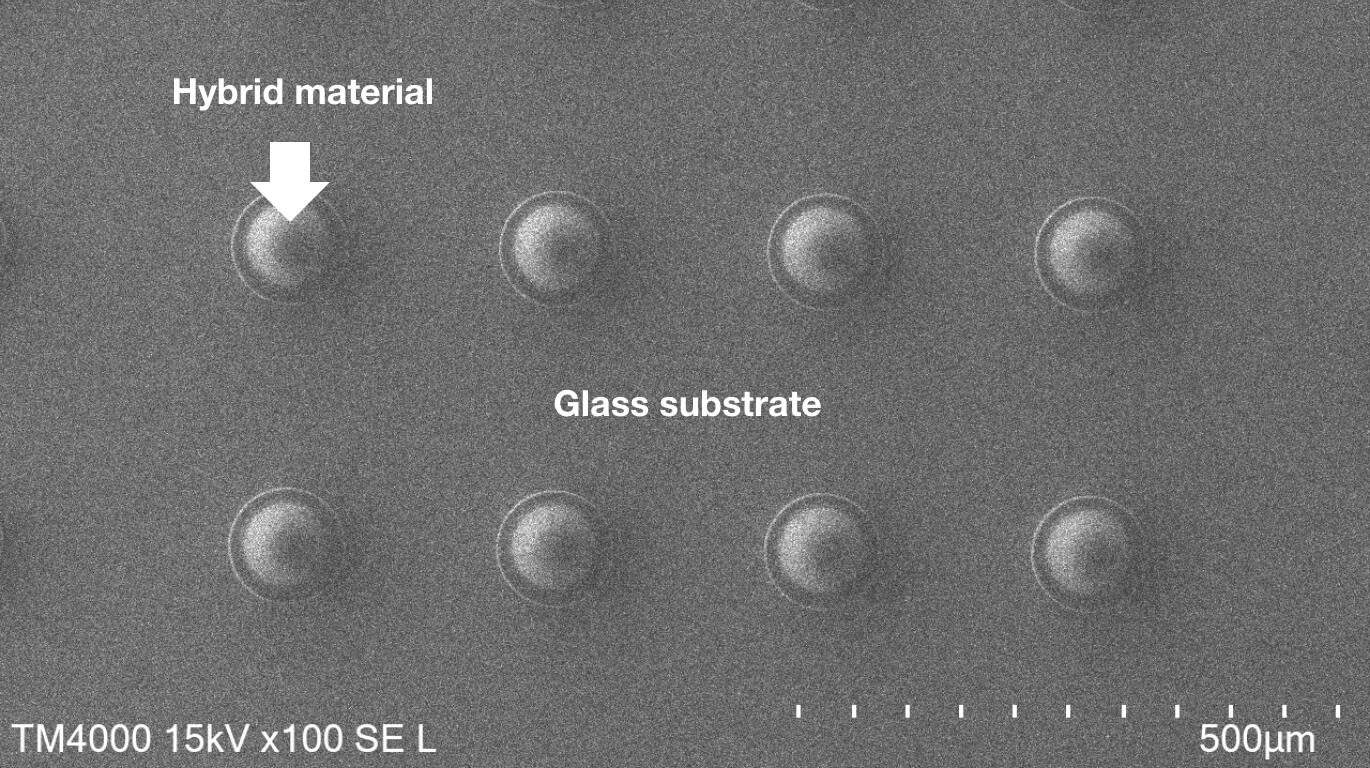
Formation of partial microstructure
Coexistence of quality and productivity
NSG’s micro optical elements achieve both environmental resistance and mass-productivity by using the organic‐inorganic hybrid material with good environmental resistance and the imprinting technology with good workability. As we produce the structure on substrates up to 8 inches using molds, we are capable of stably producing large amount of optical elements in the desired forms.
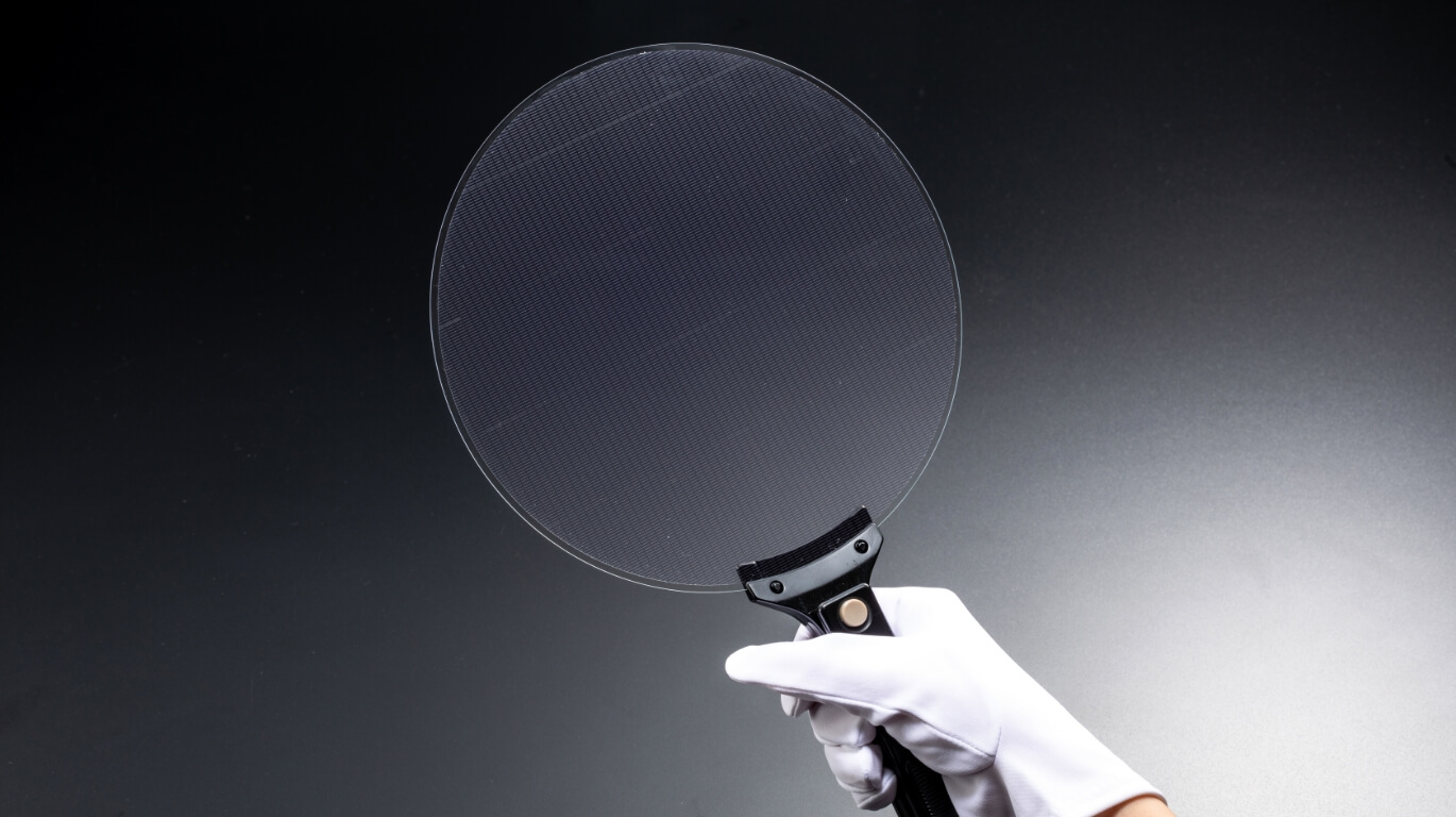
8 inch wafer
Product data
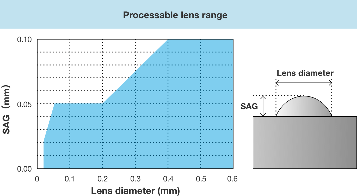
(1) We produce molds using the processing methods appropriate for the size and shape of the structure of each micro optical element, and we manufacture the micro optical element within the processing range shown in the figure. There are cases where we can accommodate those outside the processing range.
(2) The performance of the lenses does not change after conducting various reliability tests of the Telcordia Standard after a reflow test.
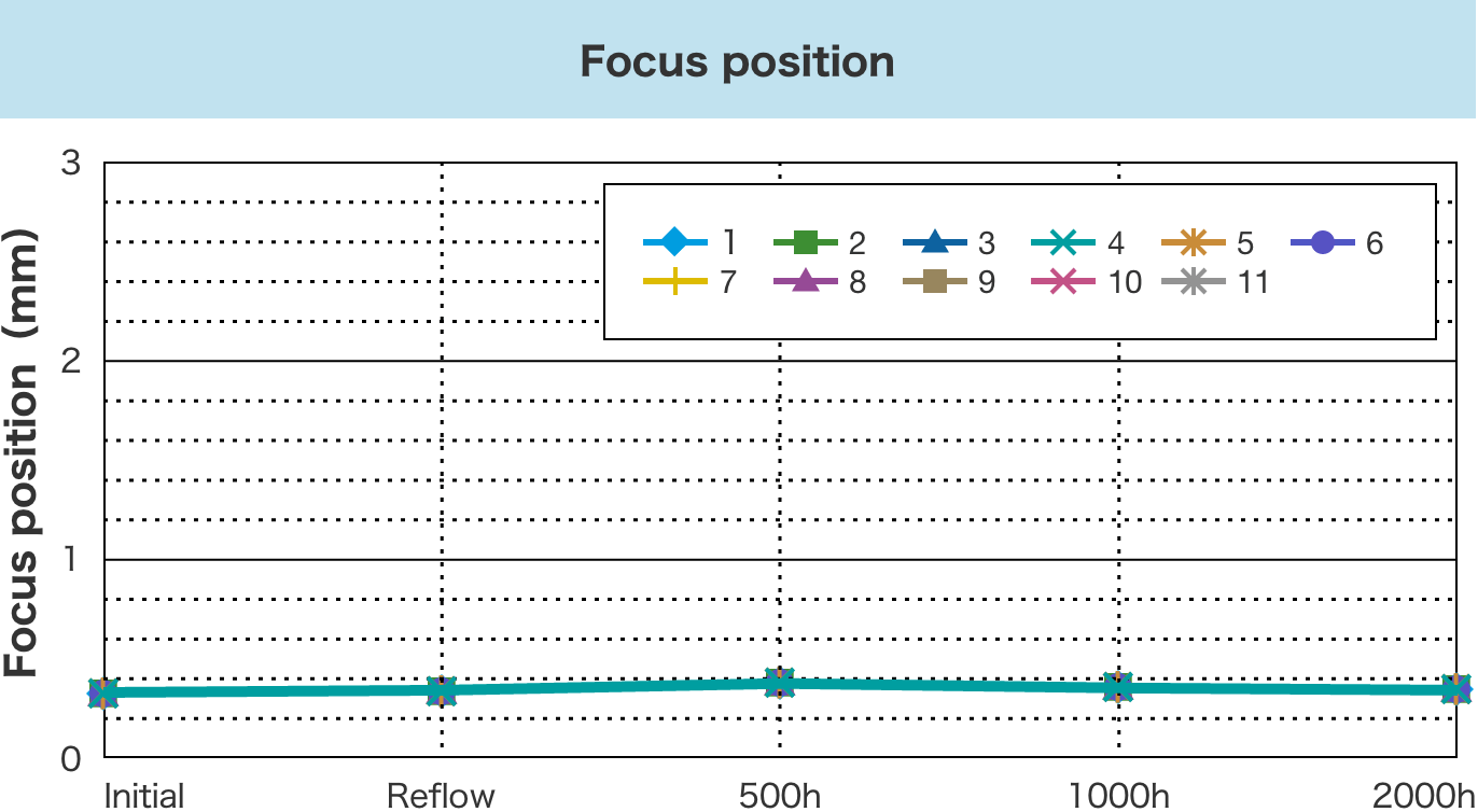
11 lenses, immediately after fabrication and after reflow processing. Damp Heat test (85°C 85%RH) after 500, 1000, and 2000 hours. (In the graph, 11 plots are overlapped.)
Glossary
Optronics
Shortened from Optical Electronics, it is also called optoelectronics. It is a technical field at the boundary between optics and electronics.
Telcordia standards
Telcordia is a research and development company that was established by the separation of the telephone business division of AT&T, an American telecommunications company. The company was originally called Bellcore when it was launched, but was sold to Telcordia Technologies. Telcordia standards are widely used as standards in the telecommunications field.
Reflow temperature
In reflow soldering, components are placed on pads with cream solder applied beforehand on the board, and the cream solder is melted in a high-temperature furnace to solder the components. The temperature at this time is generally 260°C or higher.
Imprinting technology
This is a technology that transfers and forms microstructures on a substrate using a mold with a microstructure. This is a technology with excellent mass production capability that can form microstructures accurately, repeatedly, and stably.
Damp Heat test
This is a type of environmental test, also called a constant temperature and humidity test, and is a durability test against temperature and humidity.


