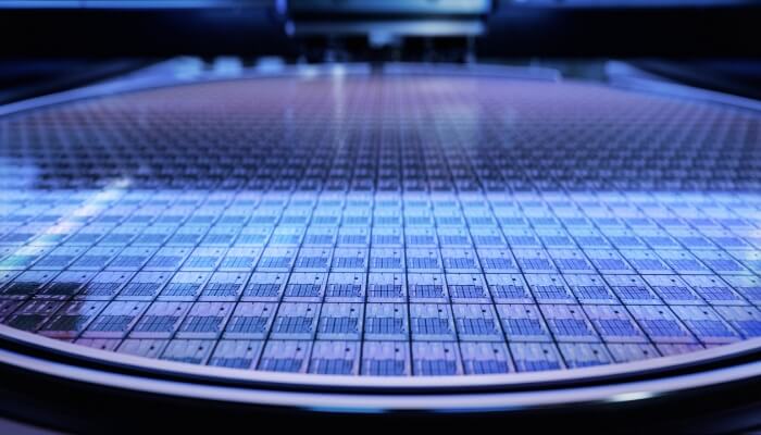
Micro Lens Array (MLA)
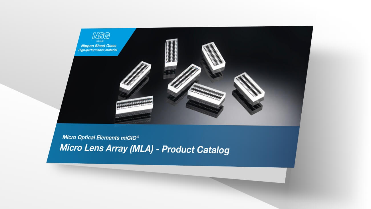
NSG's MLAs combine proprietary organic-inorganic hybrid materials with imprint technology, providing high optical performance and durability for optical communications.



Product summary
By combining NSG's proprietary sol-gel glass materials or organic-inorganic hybrid materials with imprint technology, optical components with ultra-fine structures and excellent durability can be produced. Compared with conventional methods, this process enables high-quality, cost-effective production of diffusers, diffraction gratings, DOEs and MLAs.
NSG's microlens arrays (MLAs) leverage optical design expertise developed through the development and production of optoelectronic products, enabling the manufacture of a wide variety of lens geometries. In addition, NSG provides optical design and simulation services, offering custom design, prototyping and manufacturing solutions tailored to customer requirements.
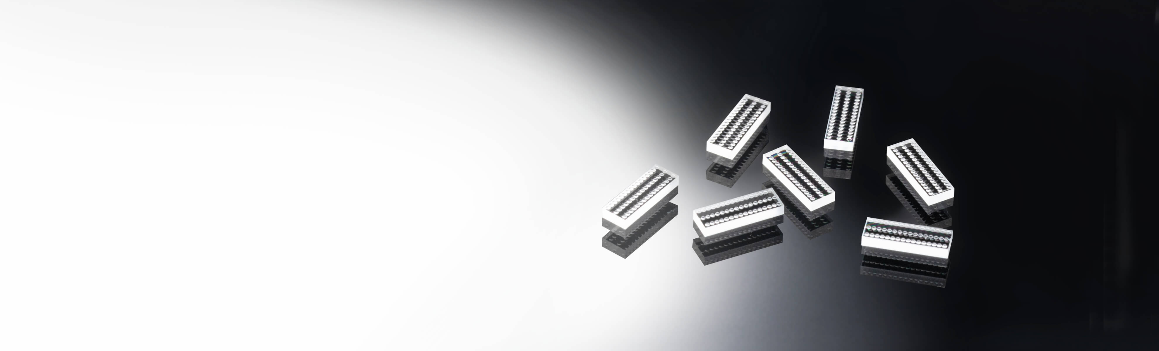
Microlens Arrays (MLAs) Utilizing NSG Proprietary Materials
For imprint molding on glass substrates, NSG can recommend the optimum material from its proprietary sol-gel glass materials and organic-inorganic hybrid materials.
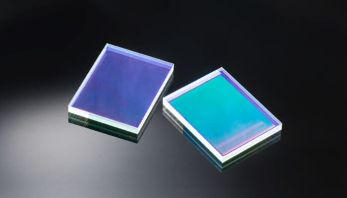
The use of NSG's proprietary organic-inorganic hybrid materials provides high reliability and heat resistance, meeting Telcordia requirements and withstanding reflow temperatures exceeding 330°C.
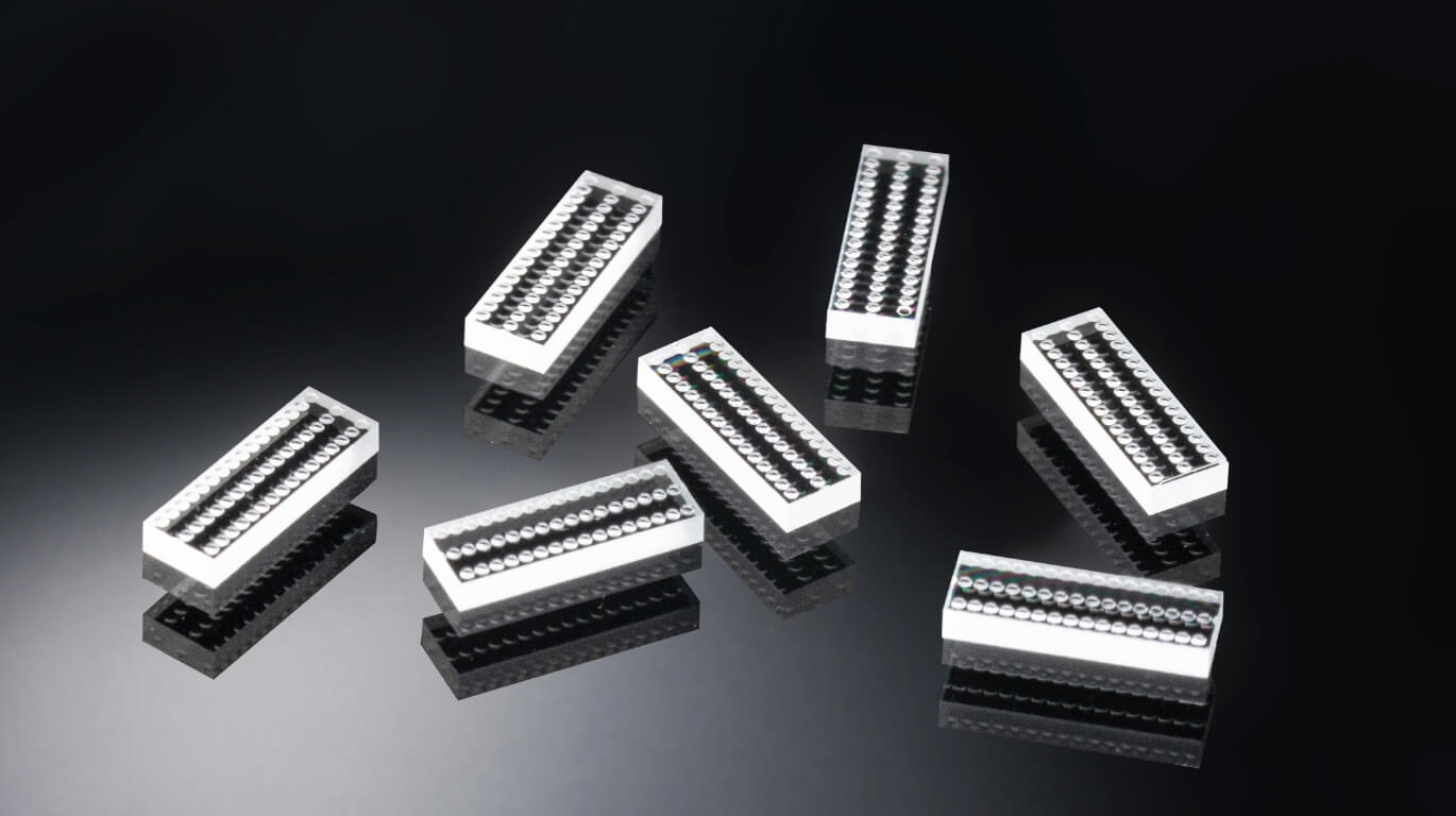
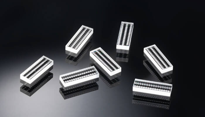
Appearance of Microlens Arrays (MLAs)
Microlens Arrays (MLAs) for Demanding Precision Requirements
By replicating precision molds fabricated using laser writing technology, NSG can produce microlens arrays (MLAs) featuring a wide variety of lens geometries, including spherical lenses, aspherical lenses, and vortex lenses.
These MLAs are suitable for applications requiring demanding optical precision, including optical communications. In addition, NSG provides optical design and simulation services, offering integrated support from optical design through manufacturing to deliver the optimum MLA solution for each application.
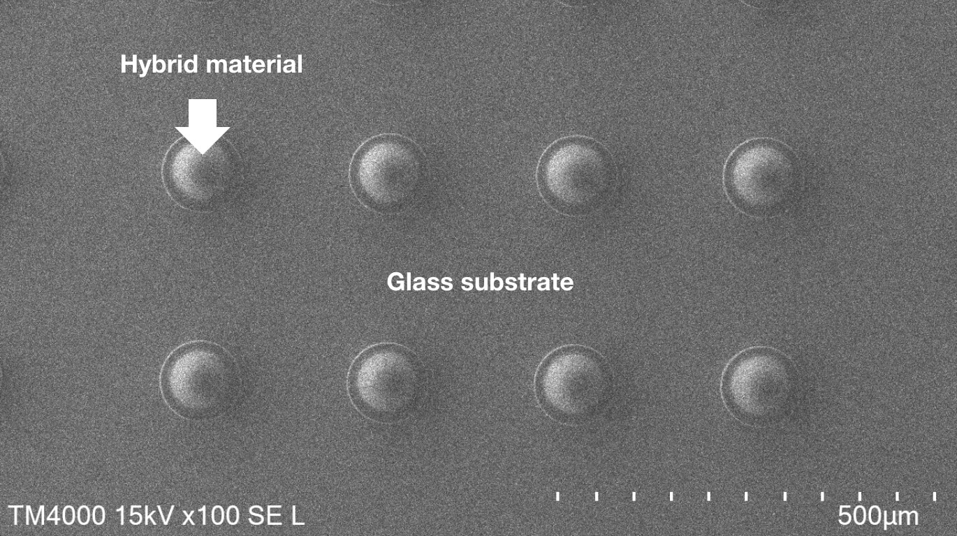
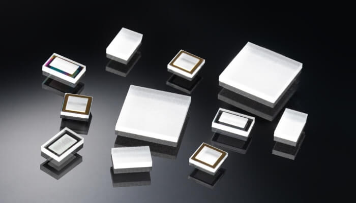
Selective Formation of Microstructures
Meeting the Precision Requirements of Optical Connectors
NSG provides high-precision microlens arrays (MLAs) for optical connector applications through its imprint manufacturing technology.
By imprinting proprietary organic-inorganic hybrid materials, these MLAs achieve high reliability and heat resistance, meeting Telcordia requirements and withstanding reflow temperatures exceeding 330°C.

Optical Connector

Optical Transceiver
Imprint Manufacturing Process
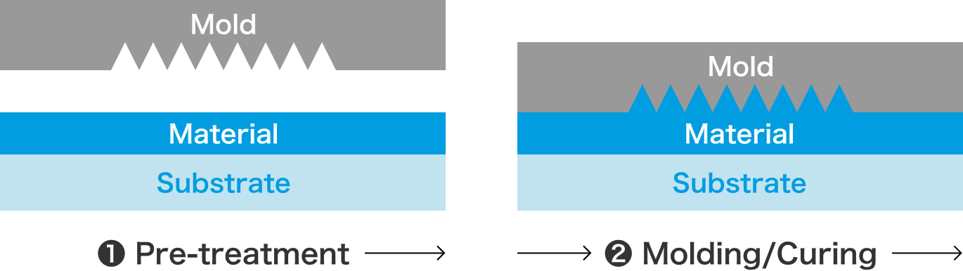
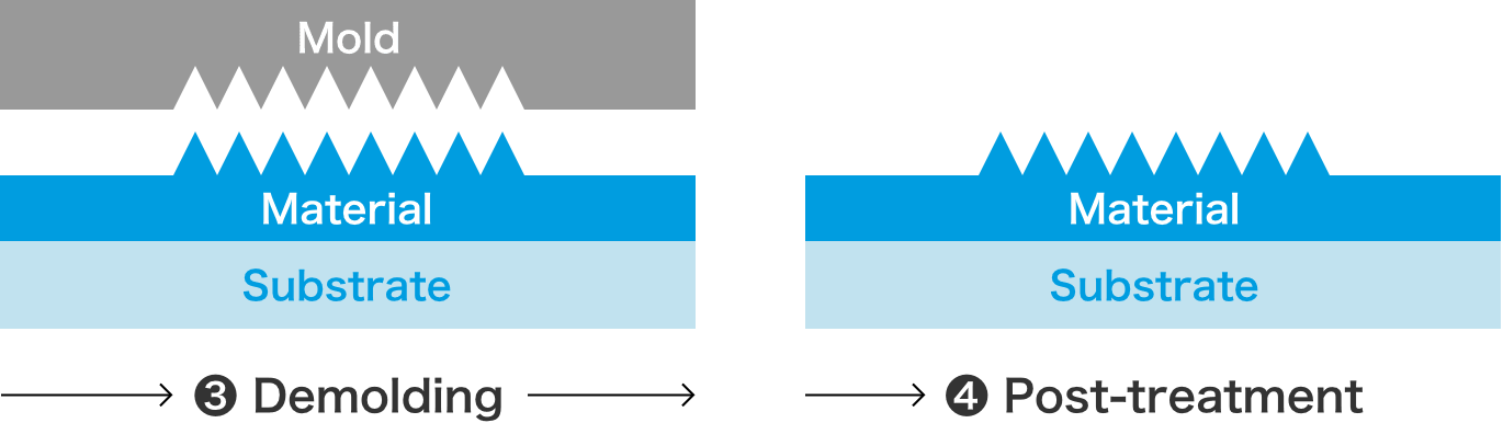
Imprinting is a manufacturing technology that uses a mold and liquid material to form components. The molding process consists of four steps: pretreatment, molding, demolding, and post-treatment.
Part of the molding process differs depending on the material used. Components are cured by thermal curing for sol-gel materials and by UV curing for organic-inorganic hybrid materials.
Precision Imprint Technology with Excellent Productivity
The imprint process using molds achieves both stable quality and excellent mass-production capability.
By utilizing high-precision molds fabricated through technologies such as laser writing and electron beam (EB) lithography, optical components can be formed simultaneously over large areas of up to 8 inches.
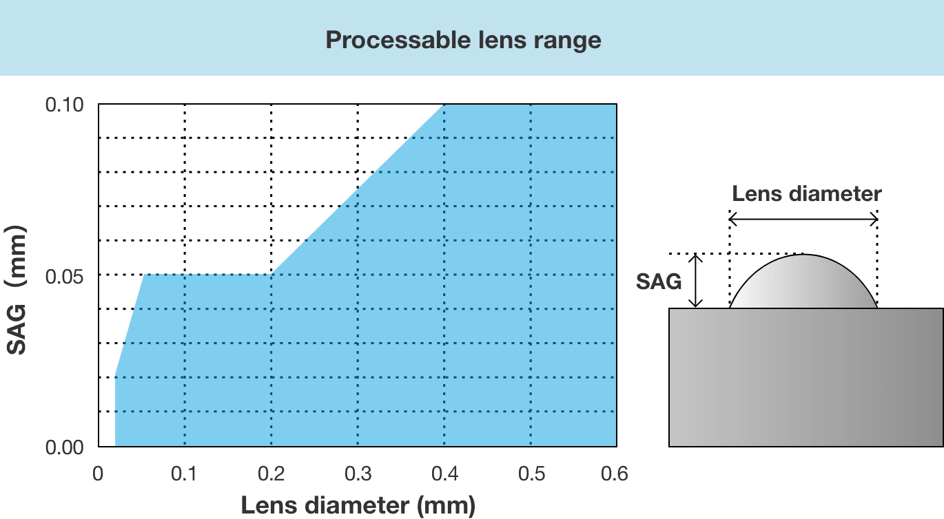
Lens Fabrication Capability Range
Molds are fabricated using the processing method best suited to the size and shape of the lens structure, and microlenses are manufactured within the fabrication range shown in the figure. Requests outside the indicated range may also be accommodated.
Lens Fabrication Capability Range
Reliability of Organic-Inorganic Hybrid Materials
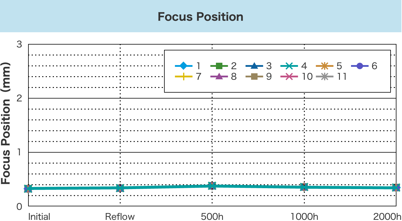
Lens performance remains unchanged even after reflow testing and subsequent reliability tests in accordance with Telcordia standards.
For eleven lenses, focal length measurements were conducted immediately after fabrication, after reflow processing, and after 500, 1,000, and 2,000 hours of Damp Heat testing (85°C, 85% RH). As shown in the graph below, the plots for all eleven lenses overlap, demonstrating their high reliability.
Measurement Results
Optical Connectors
NSG provides high-precision microlens arrays (MLAs) for optical connector applications through its imprint manufacturing technology.
By imprinting proprietary organic-inorganic hybrid materials, these MLAs achieve high reliability and heat resistance, meeting Telcordia requirements and withstanding reflow temperatures exceeding 330°C.
Optical Connector
Optical Transceiver
Automotive Applications
These products can also be used in automotive applications where durability is required, including Head-Up Displays (HUDs) and LiDAR systems.

Head-Up Display (HUD)

LiDAR
Other Applications
These products can also be used in a variety of applications, including semiconductor inspection equipment, laser modules, optical sensors, and laser cosmetic devices.
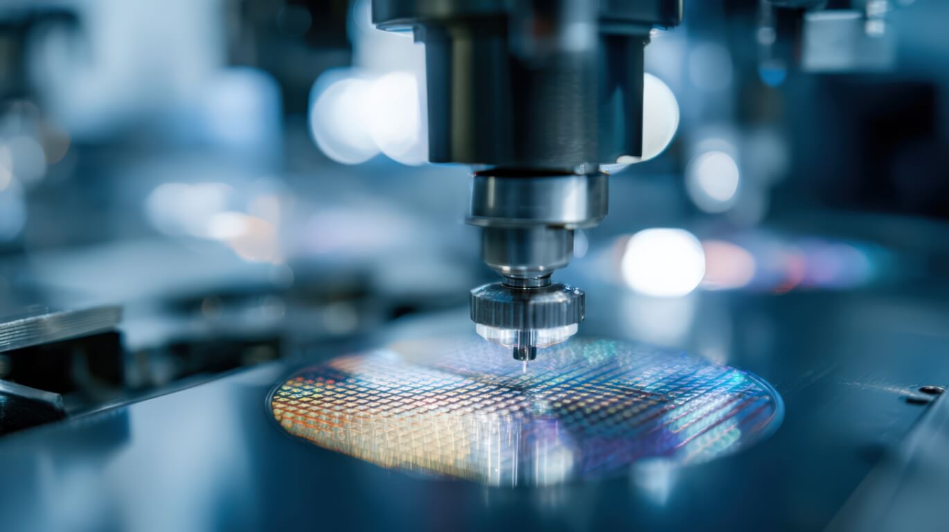
Semiconductor Inspection Equipment
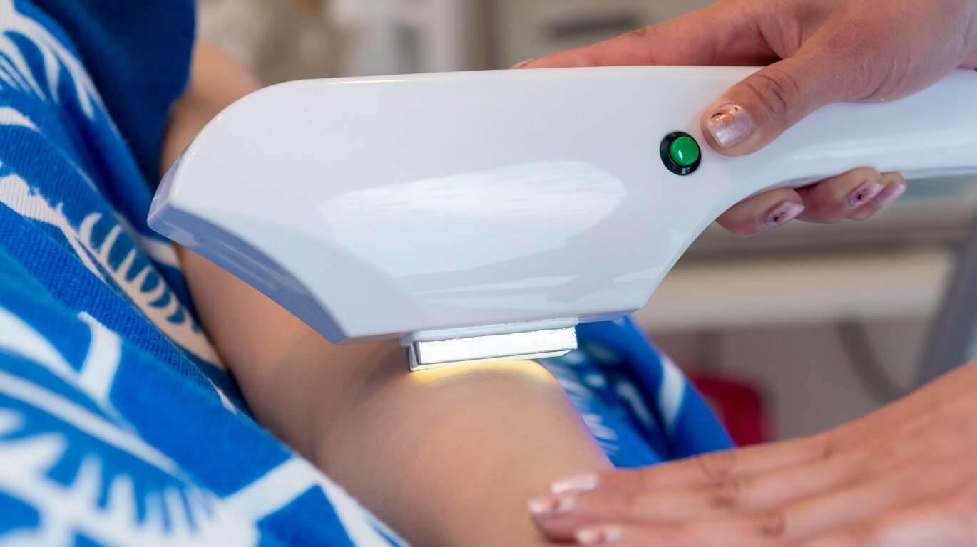
Laser Cosmetic Device
FAQ
What is a Microlens Array (MLA)?
A microlens array (MLA) is an optical component consisting of a regular arrangement of microscopic lenses and is used for applications such as light focusing and collimation.
Can anti-reflection performance be added to an MLA?
Yes. Reflection can be reduced by applying anti-reflection (AR) coatings. Various AR coating designs are available. Please contact us with your required wavelength range.
Contact us for details.Is there significant shape variation in mass production?
No. The use of mold-based imprint technology provides high replication accuracy and stable dimensional control, enabling a reliable and consistent product supply.
Can multi-channel MLAs with a large number of lenses be manufactured?
Yes. Such MLAs can be manufactured. Depending on the design requirements, there may be certain limitations, so we recommend discussing the specifications with us in advance.
Contact us for details.What is the transmission wavelength range?
The transmission wavelength range depends on the material. For sol-gel glass materials, the range is 200–2000 nm. For organic-inorganic hybrid materials, the range is 400–2000 nm.
What is reflow soldering?
Reflow soldering is a process in which components are placed on solder paste deposited on substrate pads, and the solder is melted in a high-temperature furnace to form electrical connections. The process temperature is typically above 260°C. NSG's proprietary organic-inorganic hybrid material is compatible with reflow processes (330°C for 3 minutes in a nitrogen atmosphere).
What are Telcordia standards?
Telcordia is a research and development company originally established following the separation of the telecommunications division of AT&T in the United States. It was originally known as Bellcore and later became Telcordia Technologies. Telcordia standards are widely used as industry standards in the telecommunications field. NSG's proprietary organic-inorganic hybrid materials provide excellent environmental durability.
Are samples available?
Yes. Samples may be provided depending on project details and product availability, including certain non-standard products.
Contact us for details.How much does prototyping cost?
The cost depends on the specifications. Please contact us for more information.
Contact us for details.Are samples available?
Yes. Samples may be provided depending on project details and product availability, including certain non-standard products.
Contact us for details.How long does custom design and prototyping take?
Depending on the design requirements and order timing, the typical lead time is approximately 2 to 3 months, including the design phase.
What is miGIO®?
miGIO® is the brand name for NSG's family of micro-optical products.