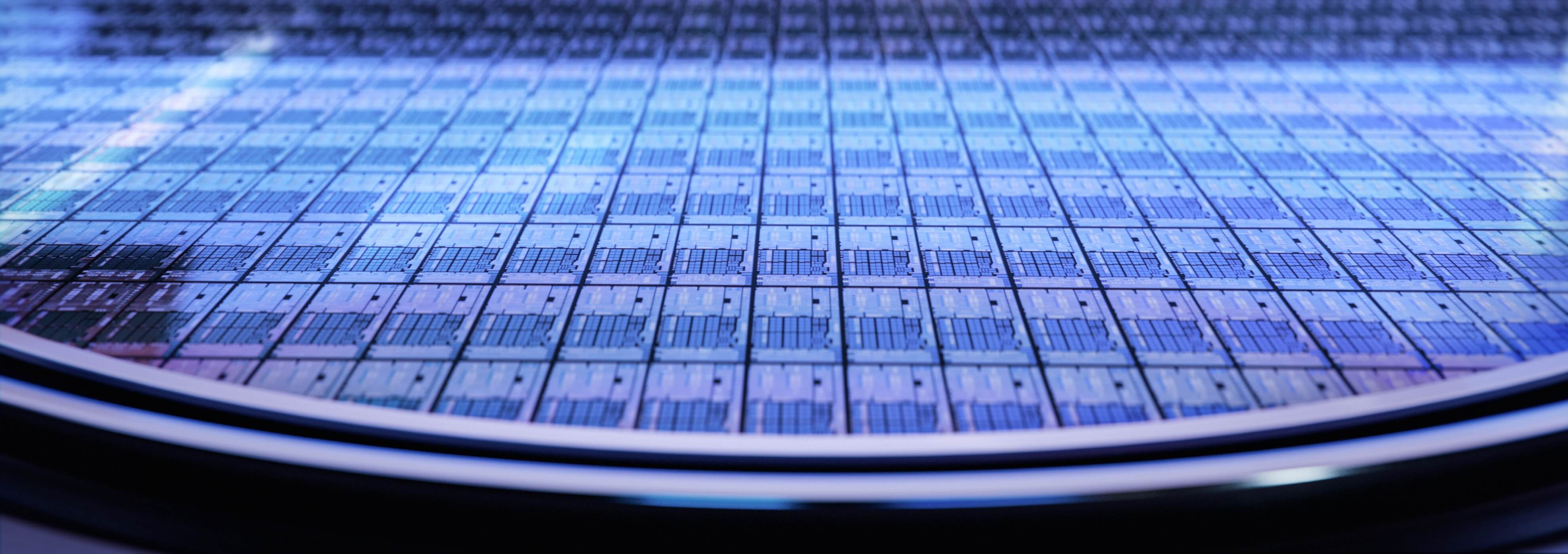
Lens on Wafer (LoW)
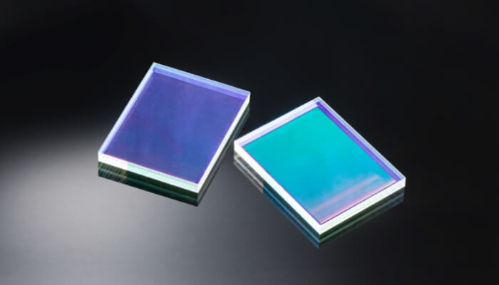
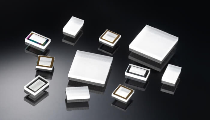
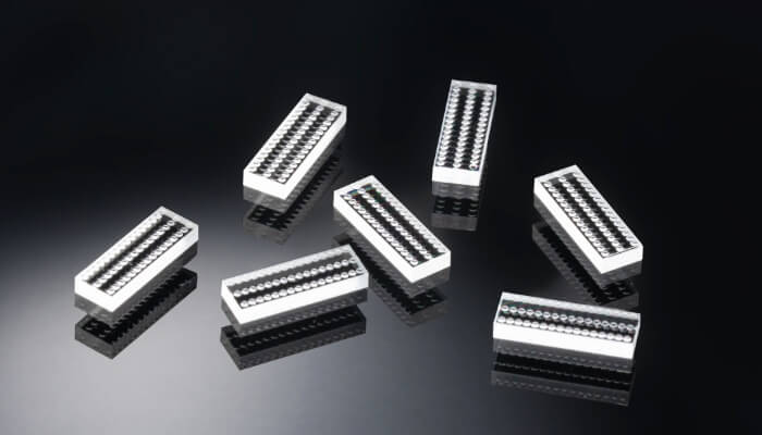
Using NSG's proprietary organic-inorganic hybrid material, lenses can be collectively formed on a wafer scale at desired locations, such as directly on optical elements of semiconductor wafers.



Product summary
By combining NSG's proprietary organic-inorganic hybrid materials with imprint technology, lenses can be formed simultaneously at desired locations across an entire semiconductor wafer, such as directly on optical elements. This wafer-level process reduces the number of alignment, assembly, and dicing steps, improving manufacturing efficiency and lowering production costs.
The use of NSG's proprietary organic-inorganic hybrid materials provides excellent reliability and heat resistance, meeting Telcordia standards and withstanding reflow temperatures exceeding 330°C.
In addition, lenses can be selectively formed only where needed while avoiding wiring areas and other structures on the wafer.

What is Lens on Wafer?
Leveraging optical component manufacturing technologies developed through the design and production of optoelectronic products, NSG can directly form lenses on semiconductor wafers.
Lenses can be selectively formed only where required while avoiding wiring areas and other structures on the wafer. In addition, the use of NSG's proprietary organic-inorganic hybrid materials provides high reliability and heat resistance, meeting Telcordia requirements and withstanding reflow temperatures exceeding 330°C.
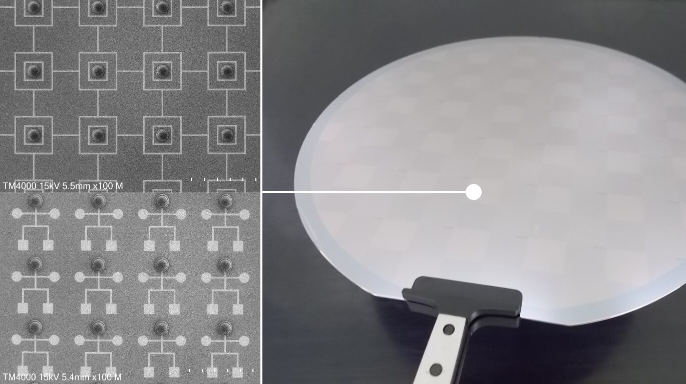
Lens on Wafer Image
Improved Efficiency and Reduced Package Thickness
Since the lenses are formed directly on the wafer with high positioning accuracy of within ±2 μm, alignment and assembly processes can be eliminated.
Direct lens formation on the wafer also contributes to thinner device packages. In addition, lens material is excluded from dicing streets, ensuring that cutting efficiency is not compromised.
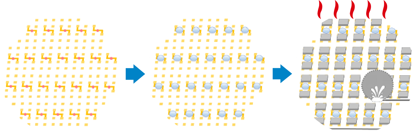
Lens on Wafer Process Flow
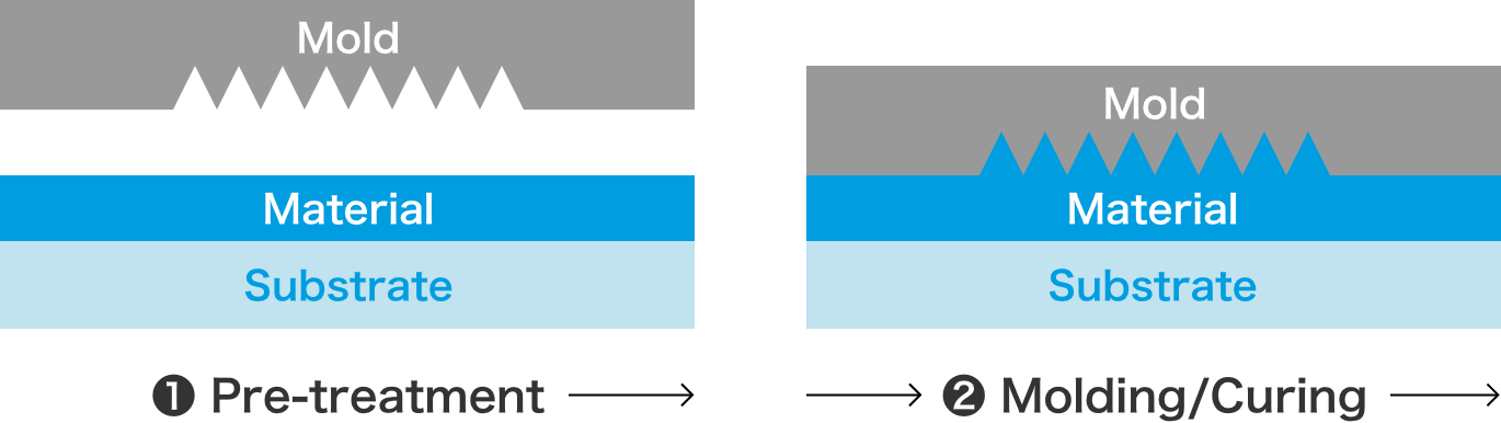
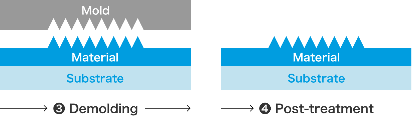
Imprint Manufacturing Process
Imprinting is a manufacturing technology that uses a mold and liquid material to form components. The molding process consists of four steps: pretreatment, molding, demolding, and post-treatment.
Part of the molding process differs depending on the material used. Components are cured by thermal curing for sol-gel materials and by UV curing for organic-inorganic hybrid materials.
Precision Imprint Technology with Excellent Productivity
The imprint process using molds achieves both stable quality and excellent mass-production capability.
By utilizing high-precision molds fabricated through technologies such as laser writing and electron beam (EB) lithography, optical components can be formed simultaneously over large areas of up to 8 inches.
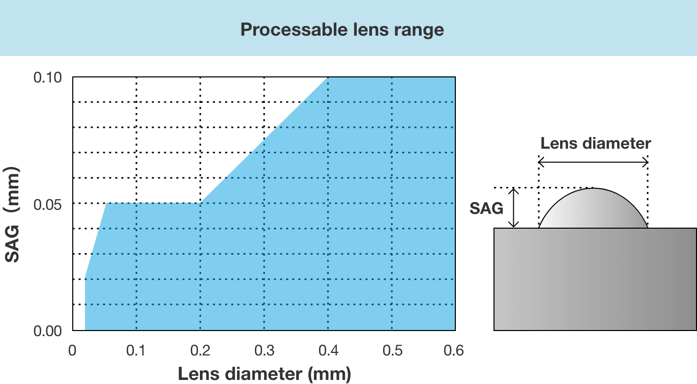
Lens Fabrication Capability Range
Molds are fabricated using the processing method best suited to the size and shape of the lens structure, and microlenses are manufactured within the fabrication range shown in the figure. Requests outside the indicated range may also be accommodated.
Lens Fabrication Capability Range
Reliability of Organic-Inorganic Hybrid Materials
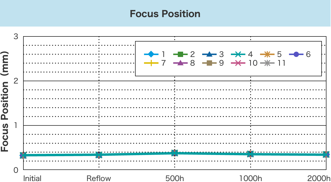
Lens performance remains unchanged even after reflow testing and subsequent reliability tests in accordance with Telcordia standards.
For eleven lenses, focal length measurements were conducted immediately after fabrication, after reflow processing, and after 500, 1,000, and 2,000 hours of Damp Heat testing (85°C, 85% RH). As shown in the graph below, the plots for all eleven lenses overlap, demonstrating their high reliability.
Measurement Results
FAQ
What is LoW?
LoW stands for Lens on Wafer.
What are the main applications?
What are the main applications?
What wafer sizes are supported for Lens on Wafer fabrication?
Currently, wafer sizes up to 8 inches are supported.
Can lenses be formed only at specific locations?
Yes. Selective local lens formation is possible, allowing lens fabrication only in required areas while avoiding wiring and other structures.
Can aspherical lenses be fabricated?
Yes. Advanced lens geometries, including aspherical lenses, can be fabricated.
What is the transmission wavelength range?
The transmission wavelength range depends on the material. For sol-gel glass materials, the range is 200–2000 nm. For organic-inorganic hybrid materials, the range is 400–2000 nm.
What is reflow soldering?
Reflow soldering is a process in which components are placed on solder paste deposited on substrate pads, and the solder is melted in a high-temperature furnace to form electrical connections. The process temperature is typically above 260°C. NSG's proprietary organic-inorganic hybrid material is compatible with reflow processes (330°C for 3 minutes in a nitrogen atmosphere).
What are Telcordia standards?
Telcordia is a research and development company originally established following the separation of the telecommunications division of AT&T in the United States. It was originally known as Bellcore and later became Telcordia Technologies. Telcordia standards are widely used as industry standards in the telecommunications field. NSG's proprietary organic-inorganic hybrid materials provide excellent environmental durability.
Are samples available?
Yes. LoW samples can be provided if the wafer is supplied by the customer.
Do I need to provide wafers when placing an order?
Yes. Customers supply the wafers, and NSG performs the imprint process at the designated locations before returning the processed wafers.
What is miGIO®?
miGIO® is the brand name for NSG's family of micro-optical products.