

Our miGIO™ micro optical elements are products achieved by combining Nippon Sheet Glass's strengths in material development, imprint manufacturing technology, and optical design capabilities.
These products feature high durability, high precision, and excellent mass production capabilities.
At Nippon Sheet Glass, we can provide comprehensive support from optical design to mass product production.
NSG's Strengths
Point 1

Materials with excellent durability
- Internally developed proprietary sol-gel glass and organic-inorganic hybrid materials
- Feature high heat resistance, chemical resistance, weather resistance, and low thermal expansion. Compatible with Telcordia standards and reflow at 330°C.
Point 2

Mass production support
- Excellent quality stability and mass productivity ensured by mold-based printing.
- Optical element formation on large surface area of up to 8 inches at once
- Optical elements on wafer alignment with high degree of accuracy of ±1μm or less. Optical element formation in necessary areas of wafer only.
Point 3
High optical design capabilities
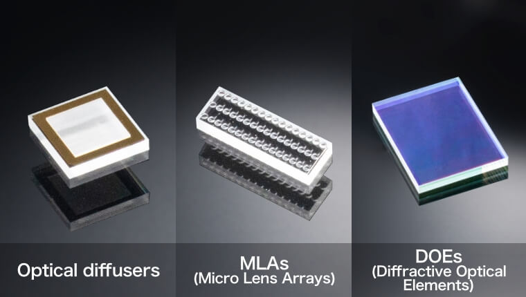
- Design and manufacture of a variety of optical elements, including Optical diffusers, DOEs (Diffractive Optical Elements), MLAs, and moth-eye structures
- Optical element design to suit your needs by Nippon Sheet Glass's optical design engineers
01
Manufacturing of individual optical elements
Features
Excellent component properties
ur micro optical elements feature high heat resistance, chemical resistance, weather resistance, and low thermal expansion. The elements are highly valued, particularly in applications requiring high heat resistance such as high-power lasers, as well as in applications demanding strict durability and reliability like medical equipment and industrial machinery.
High-precision components
With the use of molds in manufacturing, Nippon Sheet Glass mass produces high-precision components with consistent quality.
Various shapes possible
As optical components, our moldable products include MLAs, Optical diffusers, DOEs (Diffractive Optical Elements), and moth-eye structures as well as high-precision structures such as V-grooves and rectangular shapes. As inorganic imprint products, our moldable products include those with challenging features such as structures with heights of several micrometers and structures having high aspect ratios of around five. (We can achieve heights of hundreds micrometers using hybrid material.)
Product Image


Core technologies
Imprinting is a technology that uses a mold to transfer the shape of the mold onto components.
By using our uniquely developed sol-gel glass, we can form fine glass structures on substrate surfaces.
Imprint manufacturing process
Example of component specifications
The basic specifications are shown in the table below. If you have any requests regarding other structures or specifications, please don't hesitate to contact us.
| Inorganic material | |||
|---|---|---|---|
| Refractive index standard |
Refractive index high |
Silica-glass-like | |
| Purpose | Diffraction grating, DOE, Structural AR (e.g. moth-eye) etc. | ||
| Shape | Rectangle, V-groove, Blazed, Moth-eye etc. | ||
| Shape height | ~7μm | ~2μm | ~500nm |
| Aspect ratio | ~(10) | ~2 | ~1 |
| Substrate thickness | 0.1mm〜 | ||
| Substrate size | Max.120mm x 120mm | ||
| Substrate type | Fused silica/BK7/D263Teco etc. | Fused silica | |
| Refractive index | 1.4 | 1.4〜1.5 | 1.45 |
02
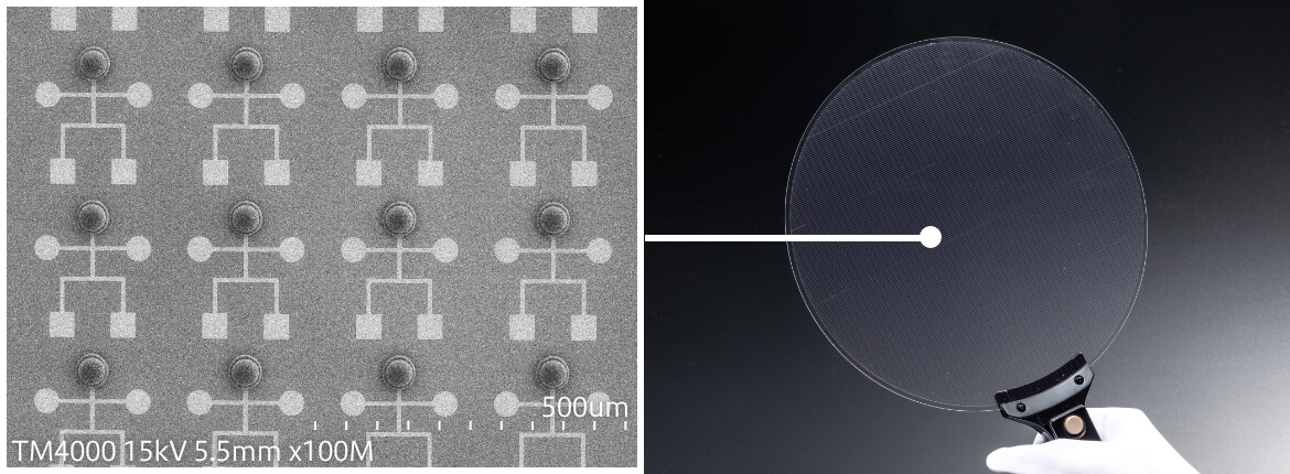
LoW (Lens-on-Wafer)
Nippon Sheet Glass's Lens on Wafer (LoW) is a type of Wafer-Level Optics (WLO) technology that forms precision, microscopic optical elements only in the targeted areas of wafer-level wiring substrates.
This technology is often used in situations where lenses and other items are directly molded onto wafer-level wiring substrates.
Features
High heat resistance
Through the development of organic-inorganic hybrid materials, our products offer high heat resistance.
Our products are compliant with Telcordia standards and accommodate reflow temperatures of 330℃ or higher.
High-precision molding only on required areas of wafer
t Nippon Sheet Glass, we can form optical elements on wafers up to 8 inches in a single process.
Optical elements on wafer alignment can be performed with a high degree of accuracy of ±1 μm or less.
We can also form optical elements in necessary areas only, avoiding regions such as wiring sections of the substrate.
Product images

Core technologies
Imprinting is a technology that uses a mold to transfer the shape of the mold onto components.
Imprint manufacturing process
Example of component specifications
The basic specifications are shown in the table below.
If you have any requests regarding other structures or specifications, please don't hesitate to contact us.
| Item | Technical capability range | Example/Remarks |
|---|---|---|
| Substrate type | Optical glass, silicon, etc. | D263, BF33, etc. |
| Substrate size | ≦Φ8" (Φ200mm) | Φ8" x t0.50mm |
| Chip size | By design | Dicing |
| Lens arrangement | By design | 12ch, 16ch, tight-lattice, etc. |
| Lens shape | Spherical, aspherical, vortex, etc. | Φ0.24, Φ0.06mm, etc. |
| Lens height | ≦0.2mm | Usually less than 0.1mm |
| Alignment accuracy | ±0.002mm | For alignment marks |
| Localized molding | Island lenses, dicing line formation, etc. | Φ0.055 x t0.03mm, pitch 0.25mm |
| Molding pitch | ≧0.09mm | Less than 0.09mm must be confirmed |
| Heat-resisting property | Reflow support | 330℃ 3min, under N2 atmosphere |
| Reliability | Telcordia GR-1211 | Passed |
03
Service
Main applications
Our technology is effective in applications that use high-power lasers and require high weather resistance and excellent reliability.
It is expected to be used in a variety of fields, including 3D sensing , LiDAR, projectors ,laser TVs, and optical communications.


Image of LoW mass production flow
We can accept work-in-progress wafers from customers, form optical elements on the wafers at Nippon Sheet Glass, and return the wafers to you.
After optical element formation, we can perform shape and property evaluations on all products using automated inspection equipment.
We can also provide inspection certificates.
Step1

Inquiry
- Application
- Shape
- Wafer size
- Quantity
- Other consultation
Step2

Interview
- NDA
- Data consultation
Step3

Order
- Specification determination
- Estimate issuance
- Order
Step4

Manufacturing
- Data creation
- Wafer receipt
- Wafer processing
Step5

Delivery
- Evaluation data
- Wafer delivery

One-stop service from design to mass production
At Nippon Sheet Glass, we can provide comprehensive support from optical design to mass production.
In addition to element manufacturing, we can also handle additional processing such as AR coating on element surfaces.
Design

Optical design
Structural design
Mold

Machining
Laser patterning
EB patterning
Proprietary materials
High precision
High durability
Large mold capabilities
Lens

High form accuracy
High intimacy
Low residual stress
High reliability
Reflow resistance
Low water absorption
Chemical resistance
Molding

Alignment accuracy
Thickness control
On target
lithography
Double-side molding
Handling

Functional wafer
Substrate with wiring pattern
Thin substrate
Weak substrate
8 inch wafer
Incidental processing

Film deposition
Cutting
Spin cleaning
Examination

Optical properties
Positional accuracy
Thickness
Appearance
Auto inspection
Mapping
Design
NSG can provide services from optical design and structural design according to various required specifications.
Mold
NSG manufacture molds using the most suitable method for your specifications. High-precision molds are suitable for mass production because they can be made in large sizes and have excellent durability.
Lens
NSG proprietary organic-inorganic hybrid materials can be transferred with high shape accuracy and have excellent durability, including reflow heat resistance exceeding 330℃.
Molding
Lenses and other optical elements are formed on various substrates such as glass and semiconductors. It is possible to form lenses with controlled alignment or on-target, and also to freely set locations where resin is not placed.
Handling
Even patterned functional wafers and thin, easily broken substrates can be protected and processed.
Incidental processing
NSG also perform incidental processing such as film deposition, cutting, and cleaning upon request.
Examination
Key inspection items such as optical properties, positional accuracy, thickness, and appearance can be evaluated and results mapped using automated inspection equipment.
Contact NSG for consultation
NSG's micro-optical elements have evolved through market needs and customer requests.
No matter how challenging the requirements, we will find solutions through technology and provide the best solutions to benefit humanity and society.
Please don't hesitate to contact NSG to discuss your needs.